GAP(111)B-SE Surface for TMD epitaxial growth
Résumé
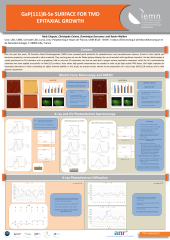
Over the past few years, 2D-Transition Metal Dichalcogenides (TMDs) have revealed great potential for optoelectronics and nanoelectronics devices, thanks to their exceptional properties, not encountered in other materials. They can be grown by van der Waals epitaxy allowing the use of materials with significant mismatch. Van der Waals epitaxy is usually performed on 2D substrates such as graphene, hBN or mica but 3D substrates can also be used after a proper surface passivation treatment, which for III-V semiconductor substrates has been applied successfully on GaAs(111)B surfaces. Since rather high growth temperatures are needed in order to get high quality-TMD layers [1], GaP might represent an interesting alternative to GaAs considering its higher thermal stability. In this study, we present results relative to the preparation of n and p-type GaP(111)B surfaces and to their Selenium passivation.
Domaines
Physique [physics]
Fichier principal
 poster GDR final.pdf (1.41 Mo)
Télécharger le fichier
GDR Howdy 2022 Chapuis abstract final.pdf (512.94 Ko)
Télécharger le fichier
poster GDR final.pdf (1.41 Mo)
Télécharger le fichier
GDR Howdy 2022 Chapuis abstract final.pdf (512.94 Ko)
Télécharger le fichier
Origine : Fichiers produits par l'(les) auteur(s)
Origine : Fichiers produits par l'(les) auteur(s)

